

This project started on February 13th, 2017, and was completed on May 18th, 2017. It involved five students:
The goal is to build an electronic device that is capable of filtering the frequencies of an audio signal from 20 Hz to 20 kHz across 16 channels, and display the level of each channel on a corresponding 10-segment bargraph. Before we dive into this project, you may want to watch a demonstration of the finalized device:
The schematics, layout files, and Gerber files are available for download here.
From Fourier's theorem, any time-dependent signal f(t) can be written as a superposition of imaginary exponentials:
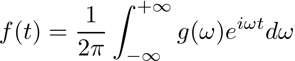
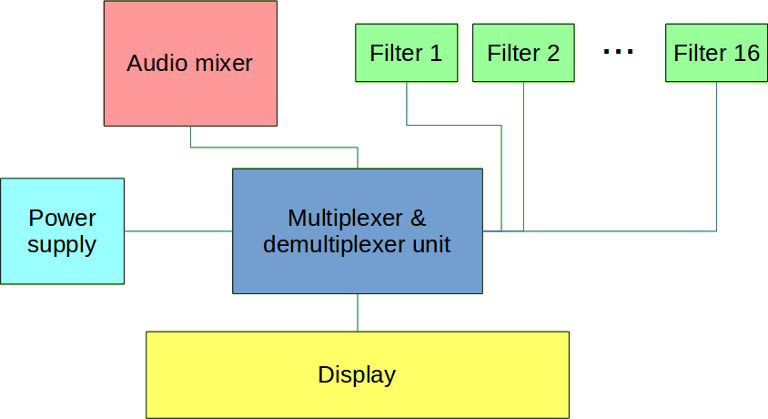
Here, ω is the angular frequency of a given exponential, g(ω) is its (complex) amplitude and is called the “spectrum” of the signal. Thus, the goal of our project is to build a device that displays a discretized version of the spectrum. The figure below shows the global diagram:
If you are not comfortabable with complex impedances, watch this tutorial.
If you are not comfortabable with operational amplifiers, watch this tutorial.
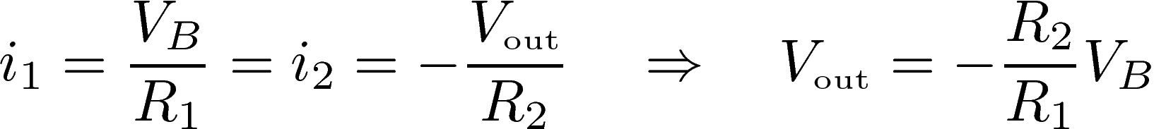
We use the following circuit:

We want to determine the complex voltage gain G=Vout/Vin. To this end, we start by writing Kirchhoff's junction rule at points A and B:

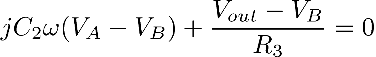
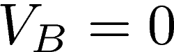
The feedback between the output of the op-amp and its inverting input guarantees that it works in the linear regime. As a result, the op-amp automatically adjusts its output in order to keep a zero potential at point B:
Substituting this value into the two Kirchhoff's equations above, and solving for Vout/Vin, we obtain the complex gain:

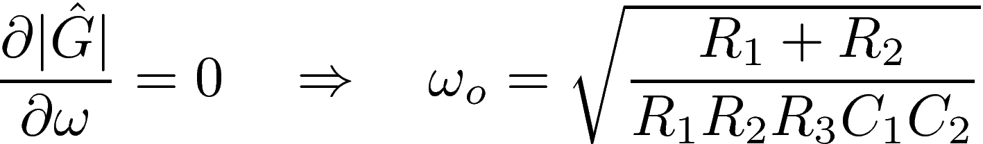
It is clear from the expression above that G vanishes only for ω=0 and ω=+∞. As a result, the circuit is a band-pass filter, as required. The resonant frequency ωo is obtained by setting the derivative of the gain's modulous to zero, and keeping only the real and positive solution for the frequency:
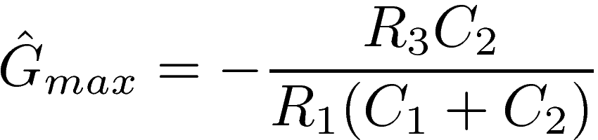
Substituting the resonant frequency into the expression for the gain, we obtain the maximum gain, which is real and negative, and implies that the output signal is in opposite phase with the input signal:
Something that is crucial to consider is the bandwidth Δω=ω+-ω- of the filter, where ω+ and ω- are the cutoff frequencies. These cutoff frequencies are defined as those for which the power gain is half of the maximum power gain. In terms of the voltage gain, this implies:
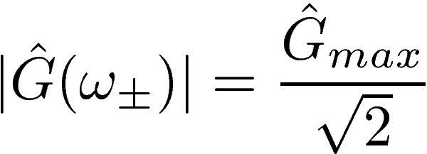
Taking the square of the above equation and substituting the expression for G(ω), we obtain a 4th degree equation for ω±:
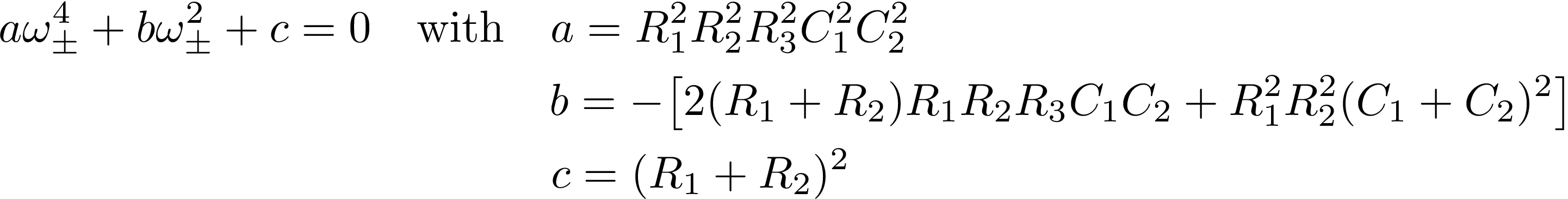
This equation is easily solved for ω±2, and the solution for ω± is given by taking the positive root. The resulting expression for the bandwidth Δω seems to be complicated:

However, it “miraculously” simplifies well. This can be easily seen by calculating first the square of the bandwidth, then taking the square root of it:

The figure below summarizes the features of the filter:
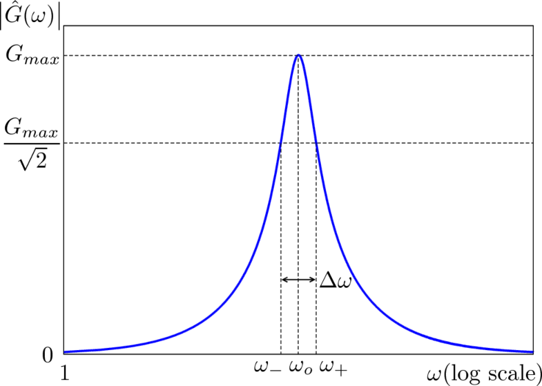
In order to characterize how selective the filter is, we define the Q-factor as the ratio of the resonant frequency to the bandwidth:
With this definition, the higher the Q-factor, the more selective the filter. The Q-factor must be high enough so that only one bargraph displays a maximum level when a single frequency is injected, but not too high otherwise no signal will be displayed if the frequency falls between the resonant frequencies of two neighboring bargraphs. Our choice for a suitable Q-factor is explained below, as well as our choice for the 16 resonant frequencies. The maximum gain can be arbitrarily chosen to be unity. Assuming that a choice for ωo, Gmax, and Q has been made, and introducing the linear resonant frequency Fo=ωo/2π which is more human-friendly than the angular frequency ωo, we can determine the values of the resistors R1, R2, R3 by inverting the expressions above:

The values for C1 and C2 can be freely chosen in order to obtain reasonable values for R1, R2, R3. We want these values to be large enough in order to avoid excessively large currents, but not too large in order to keep a good signal/noise ratio.
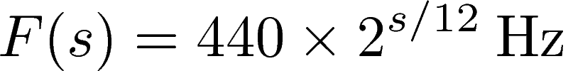
As already mentioned, the gain can be arbitrarily set to unity, Gmax=1, since the audio mixer allows to adjust the level of the input signal (hence the level of the signal that comes out of the filters). For the resonant frequencies, we have to consider the fact that the perception of sounds by humans as “higher” or “lower”, the so-called “pitch”, is not directly proportional to the frequency. Instead, it is observed that the pitch increases by a constant step when the frequency is multiplied by a constant number. In order to determine the exact relationship between pitch and frequency, it is common to define the pitch associated to a frequency of 440Hz as a A4. Multiplying the frequency by two, 880Hz, is perceived as a A5, while dividing it by two, 220Hz, is perceived as a A3. The pitch change between Ai and Ai+1 is called an “octave” and is divided into 12 semitones. It follows that the frequency of a pitch that corresponds to s semitones above (s>0) or below (s<0) the A4 reference pitch is given by:
Thus, the frequency increases exponentially with the pitch as perceived by humans. We want the resonant frequencies to be evenly distributed from 20Hz to 20kHz in terms of pitch. In other words, we want the number of semitones between the resonant frequencies to be a constant. In order to determine this constant, we start by inverting the above equation in order to obtain the number of semitones above or below A4 that correspond to a given frequency F:
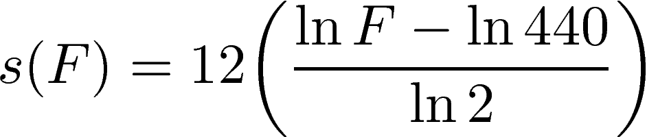
We want to divide the range of semitones between 20Hz and 20kHz into 15 constant intervals. Thus the number of semitones no between the resonant frequencies must be:

It follows that the resonant frequency Fk of the kth filter is given by:

As a result, the resonant frequencies are:
| Filter # | 1 | 2 | 3 | 4 | 5 | 6 | 7 | 8 | 9 | 10 | 11 | 12 | 13 | 14 | 15 | 16 |
|---|---|---|---|---|---|---|---|---|---|---|---|---|---|---|---|---|
| Frequency (Hz) | 20.0 | 31.7 | 50.2 | 79.6 | 126 | 200 | 317 | 502 | 796 | 1.26k | 2.00k | 3.17k | 5.02k | 7.96k | 12.6k | 20.0k |
Finally, we need to determine a suitable Q-factor. We don't want the bandwidths of neighboring filters to overlap otherwise the filters would respond to the same frequencies, and we don't want to leave any gap between those bandwiths otherwise some frequencies would not be detected. Thus, it makes sense to choose the bandwidths so that they touch each other. So, the bandwidth ΔFk of filter k must be equal to Fk+1/2-Fk-1/2. As a result, the Q-factor is the same for all filters and given by:

Having chosen the gain, the Q-factor, and the resonant frequencies, we can finally determine suitables values for C1, C2, R1, R2, R3:
| Calculated | Actual value | |||||||
|---|---|---|---|---|---|---|---|---|
| C1 (F) | C2 (F) | R1 (Ω) | R2 (Ω) | R3 (Ω) | R1 (Ω) | R2 (Ω) | R3 (Ω) | |
| Filter 1 | 100n | 100n | 171k | 20.8k | 342k | 180k | 20k | 330k |
| Filter 2 | 100n | 100n | 108k | 13.1k | 216k | 110k | 13k | 220k |
| Filter 3 | 100n | 100n | 68.2k | 8.27k | 136k | 68k | 8.2k | 130k |
| Filter 4 | 100n | 100n | 43.0k | 5.21k | 86.0k | 43k | 5.1k | 82k |
| Filter 5 | 100n | 100n | 27.2k | 3.29k | 54.3k | 27k | 3.3k | 56k |
| Filter 6 | 100n | 100n | 17.1k | 2.08k | 34.2k | 18k | 2k | 33k |
| Filter 7 | 100n | 100n | 10.8k | 1.31k | 21.6k | 11k | 1.3k | 22k |
| Filter 8 | 10n | 10n | 68.2k | 8.27k | 136k | 68k | 8.2k | 130k |
| Filter 9 | 10n | 10n | 43.0k | 5.21k | 86.0k | 43k | 5.1k | 82k |
| Filter 10 | 10n | 10n | 27.2k | 3.29k | 54.3k | 27k | 3.3k | 56k |
| Filter 11 | 10n | 10n | 17.1k | 2.08k | 34.2k | 18k | 2k | 33k |
| Filter 12 | 10n | 10n | 10.8k | 1.31k | 21.6k | 11k | 1.3k | 22k |
| Filter 13 | 1n | 1n | 68.2k | 8.27k | 136k | 68k | 8.2k | 130k |
| Filter 14 | 1n | 1n | 43.0k | 5.21k | 86.0k | 43k | 5.1k | 82k |
| Filter 15 | 1n | 1n | 27.2k | 3.29k | 54.3k | 27k | 3.3k | 56k |
| Filter 16 | 1n | 1n | 17.1k | 2.08k | 34.2k | 18k | 2k | 33k |
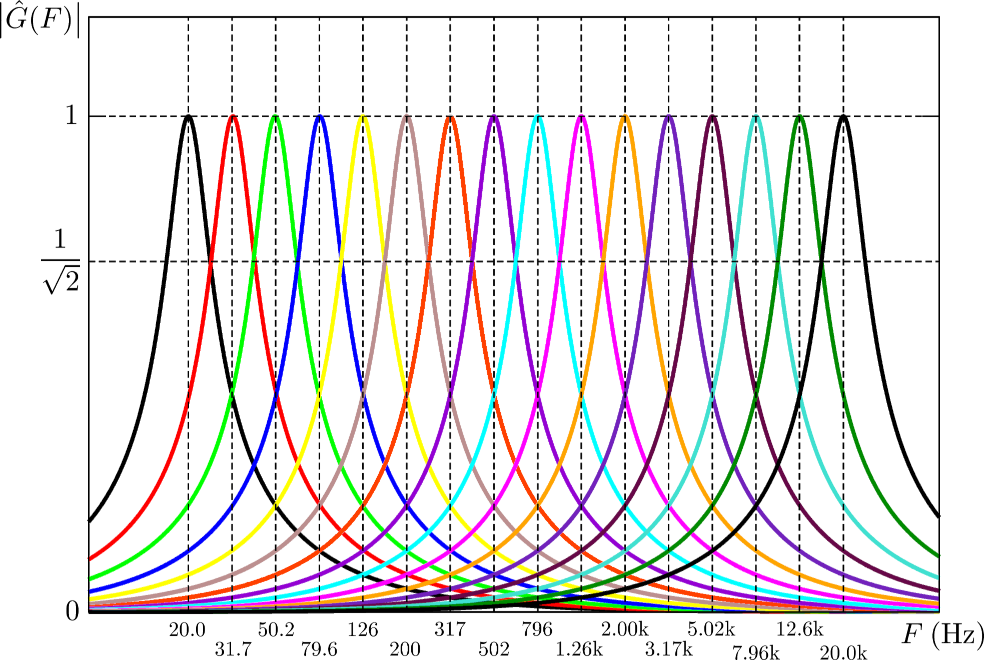
The figure below shows the gain of the 16 filters.
The output of each filter is sent through a peak detector that converts the AC signal into a DC signal, and generates a time-delayed decay in order to ease the visualization of the signal. This is realized with the circuit below:

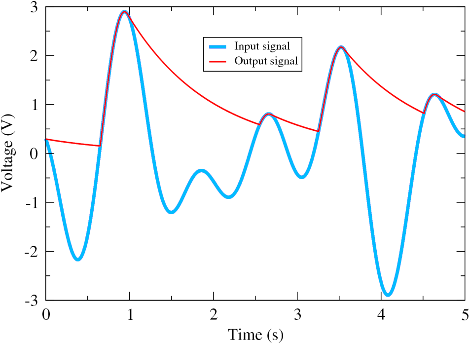
If the input voltage is higher than the output voltage, then the op-amp adjusts its output in order to forward-polarize the diode and keep the circuit's output at the same potential as the input, which results in the capacitor being instantly charged with the same value as the input voltage. If the input voltage is lower than the output voltage, then the op-amp saturates to -Vsat and the diode is reverse-polarized, blocking any current from flowing. Thus the capacitor and resistor are decoupled from the rest of the circuit and the capacitor discharges across the resistor. As a result, the output voltage decreases exponentially with a time constant RoCo. Therefore, the op-amp and the diode act as an ideal diode with no threshold and a vertical I(V) characteristics. As a result, the circuit keeps a short-time memory of the input signal's peak voltage.
In our case, we want the memory of the peak voltage to drop down to half its initial value in about one second, which implies to choose the resistor and the capacitor such that RoColn(2)=1. For example, we can choose Ro=1.2MΩ and Co=1μF. The figure below shows an example of response to an arbitrary input signal:
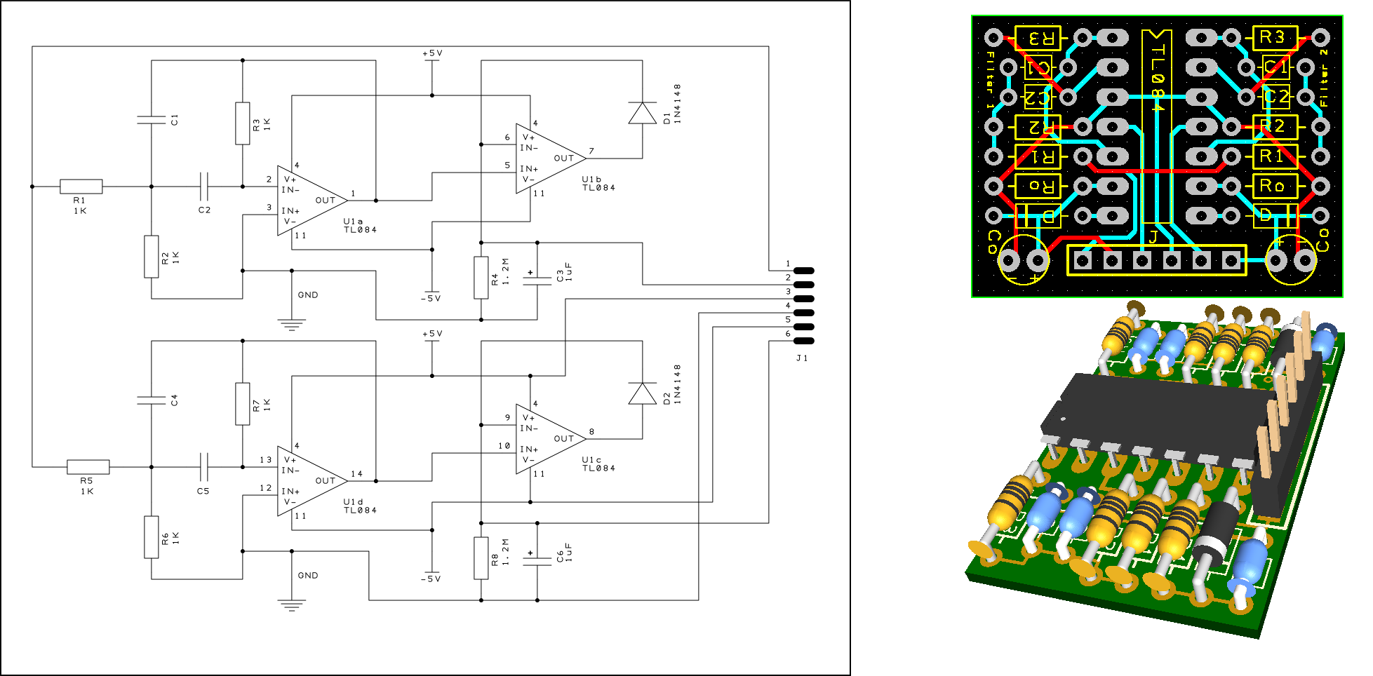
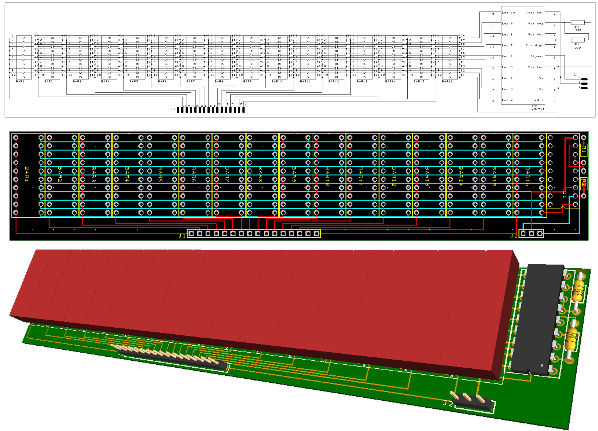
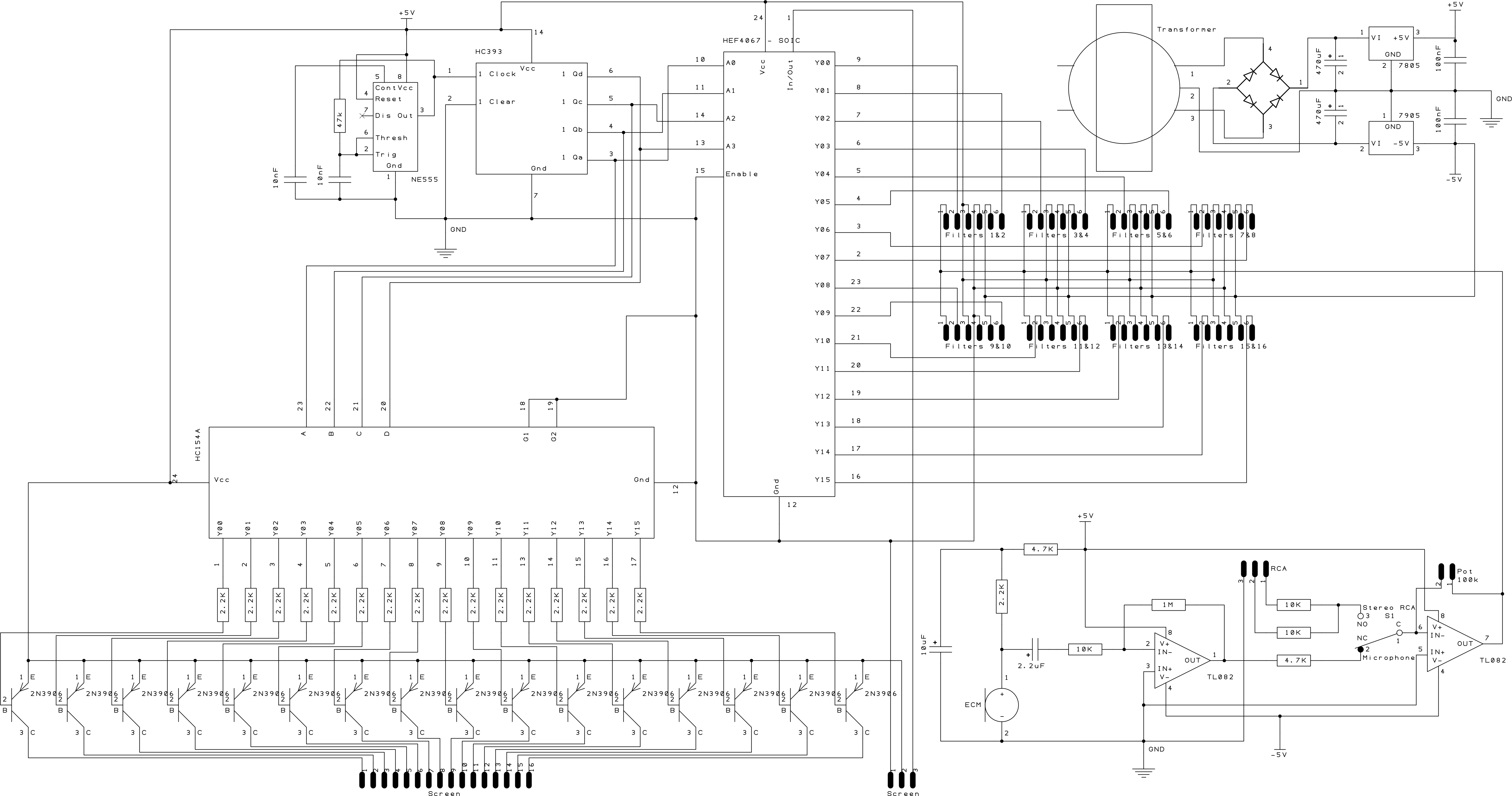
For the realization, it is interesting to keep the filters with their peak detectors on separate circuit boards, so that they can be easily replaced by others with different characteristics if needed. Here, a good solution is to make use of the TL084 integrated circuit that includes four op-amps, allowing us to incorporate two filters with their peak detectors. The figure below shows the final schematic of the circuit, the corresponding PCB image, and a 3D preview of the assembled circuit board. The final device will include 8 circuit boards like this.
The output level of each peak detector needs to be converted into a number of bargraph segments to be turned on. We want the first LED segment to be on when the signal level is greater than a given reference potential V1, the two first LED segments to be on when the signal level is greater than a given reference potential V2, ..., and all ten segments to be on when the signal level is greater than a given reference potential V10. This can be done by using a so-called “LED driver” composed of op-amps used as “comparators”. The figure below shows the circuit:

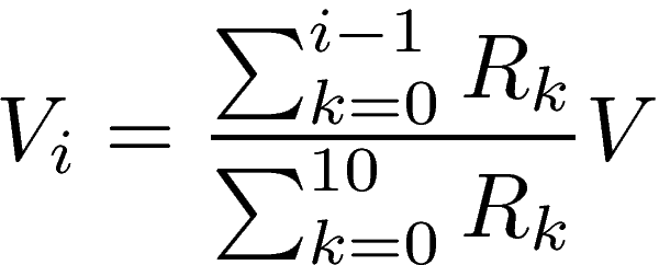
The reference potentials V1, V2, ..., V10 are determined by choosing suitable values for the resistors R0, R1, R2, ..., R10, which constitute a voltage divider. The reference potential Vi is easily determined as:
Each reference potential Vi is connected to the non-inverting input of the corresponding op-amp. Because of the absence of feedback between the output and the inverting input of the op-amps, they work in the non-linear regime. As a result, the ith op-amp saturates to a high potential as long as the input signal Vsig remains lower than Vi. This prevents any current from flowing across the ith LED segment, which remains off. When the input signal Vsig becomes greater than Vi, the op-amp saturates to a low potential. This forward polarizes the LED which comes on. The 220Ω resistors are there to avoid excessive currents in the LED segments.
One problem with the above circuit is that, in addition to the LED segments, it includes 10 op-amps and 21 resistors. We need one LED driver for each of the 16 bargraphs, which would require a total of 160 op-amps and 336 resistors. In order to solve this problem, we use the LM3914 integrated circuit which implements the above circuit (without the LEDs) in a small 18-pin dual in-line package (DIP). Still, we need in principle 16 LM3914 integrated circuits, one for each bargraph. In order to reduce further the number of components, we use a multiplexing/demultiplexing technique. This technique consists in controlling only one bargraph at a time while the others are turned off, and switching sufficiently fast to the next bargraph so that we have the impression that they are all on at the same time. As a result, only one LM3914 is needed, which is connected to the cathodes of the 16 bargraphs. The anodes are controlled separately by the main board that takes care of turning on only one bargraph at a time, while sending the output signal of the corresponding filter and peak detector to the LM3914. The details on how the multiplexer/demultiplexer unit achieves this are given below. The figure below shows the final schematic of the display, the corresponding PCB image, and a 3D preview of the assembled circuit board.
The integrated circuits used in the device need a DC power supply. In particular, the op-amps must be supplied with a symmetric voltage. Here, we can choose to work with the minimum voltage of +5V, 0V, -5V that will satisfy all integrated circuits. The power supply must be able to deliver a current of 1A or more in order to make sure that there is enough current to supply all circuits and LEDs. We can use a transformer that converts the 120V AC from a wall outlet into two 6V AC sources. This is done by using a primary coil that induces an electromotive force into a secondary coil that is tapped at its center in order to divide it into two equal electromotive forces. The electromotive force induced into the secondary coil is equal to the ratio of the number of turns of the secondary to the primary. By using a ratio of 1/10, the electromotive force induced into the secondary is 12V AC, hence two times 6V AC. Then this symmetric AC voltage is converted into a symmetric DC voltage as described below. For this, we use the following circuit:

First, consider only the transformer and the bridge rectifier (the four diodes) in the above picture, and assume that no other components are connected. It is easy to see that, whether the potential difference between the secondary's terminals 1 and 2 is positive or negative, the potential at the bridge's + terminal is always positive and the potential at the potential at the - terminal is always negative (with respect to the ground). These potentials, in absolute value, are slightly less than those at the secondary terminals because of the nearly constant voltage drop across the diodes. If we add now the rest of the circuit, the large 470μF capacitors at the terminals of the bridge will charge instantly across the diodes when they are forward-polarized, and will discharge exponentially across the two regulators when the diodes are reverse-polarized. Therefore, the potential at the secondary's terminals 1 and 2, the bridge's terminals + and - without the rest of the circuit, and with the rest of the circuit take the form as shown on the figure below:
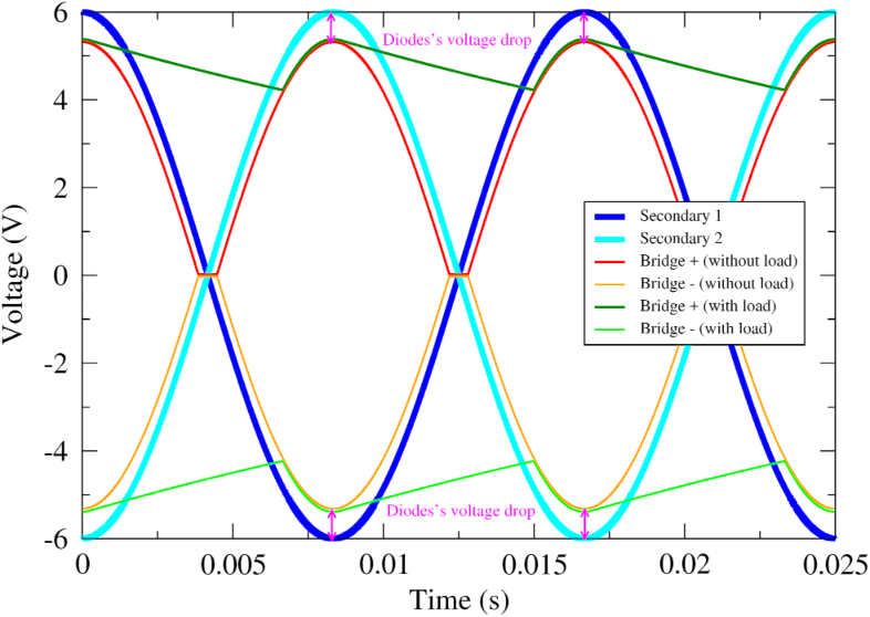
The signals present at the inputs of the two regulators (bridge + and - with load) are now sufficiently rectified so that the regulators can work properly and output constant potentials of +5V and -5V. The two 100nF capacitors are there in order to remove any remaining noise. They block the flow of DC currents, and their impedance is small for the typical high frequencies associated with noise, creating a short to kill it. Note that it would be a mistake to think that large electrolytic capacitors would be able to remove the noise better than the small 100nF capacitors, since they have (in principle) a even lower impedance. However, electrolytic capacitors have a non negligible inductance that actually makes their impedance increase at high frequencies. It is therefore necessary to use small capacitors with negligible inductance in order to filter out the noise.
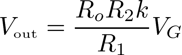
The audio mixer allows us to select the audio input from RCA connectors or from an internal microphone. For the microphone, we use an electret condenser microphone (ECM) which has the advantage of being very small. The ECM contains a piezoelectric crystal that generates an AC voltage proportional to the sound's level. The AC voltage generated is way too small for practical applications. This is why the ECM includes a field-effect transistor (FET) in order to amplify it. Consider the figure below:

The FET requires a supply voltage Vdd via a resistor Ro connected to the drain (D). The ground is connected to the source (S). The FET works in such a way that the current i that enters into the drain depends linearly on the potential VG present at the gate (G), which is the voltage generated by the piezoelectric crystal:
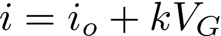
In the above equation, io is a constant current that depends on Ro and Vdd, and k is a constant coefficient. Applying Ohm's law to the resistor, we deduce the value of the potential at point A:

As a result, VA oscilates around the constant value Vdd - Roio, and the voltage VG generated by the piezoelectric crystal is amplified by a factor -Rok. For the ECM to work properly, the constructor recommends using Ro=2.2kΩ with a supply voltage Vdd between 3V and 10V. Here we will use Vdd=5V. Still, the oscillations of the voltage VA are too small and need to be amplified. Also, we need to have a signal that oscillates around zero instead of the constant value Vdd - Roio (typically between 2V and 4V), otherwise the signal will saturates when it will be amplified. This is done by connecting the above circuit to an amplifer via a decoupling capacitor, as shown below:

The decoupling capacitor Co blocks DC currents, and has a capacitance that is sufficiently large so that its impedance for frequencies above 20Hz is small compared to R1. For these frequencies, the capacitor behaves as a wire. Also, R1 is chosen sufficiently large compared to Ro so that the potential VA is unaffected by the current drawn across the capacitor, thus the above expression remains valid. As a result, only the AC part of VA goes through the capacitor, and the potential VB oscillates proportionally to VG around zero:

The feedback resistor R2 between the output of the op-amp and the inverting input guarantees that the op-amp works in the linear regime. This implies that the potential at the inverting input is the same as that at the non-inverting input, hence zero. Noting that the current i1 across R1 must be the same as the current i2 across R2, and applying Ohm's law, it follows that:
As a result, the voltage VG generated by the piezoelectric crystal is amplified again, for R2>R1, and the output voltage takes the form:
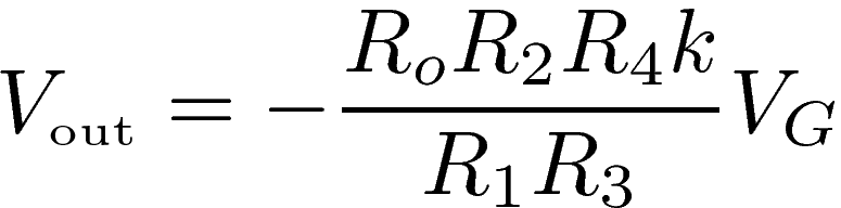
Although the values VG and k are unknown, choosing R1=10kΩ, R2=1MΩ, Co=2.2μF satisfies the conditions of validity of the above equations, and the measured output signal Vout has a level comparable to the signal's level typically present on RCA inputs. We use a switch that allows us to select between the microphone or the RCA inputs. The RCA stereo signals are mixed into a single signal that is equal to their average. Then the selected input signal needs to be amplified again or attenuated in order to fall within a level that can be displayed by the bargraphs without saturating. This is done by using another op-amp with an ajustable resistor for the feedback. The final circuit for the audio mixer is:

When the switch is up, the microphone's signal is selected and the previous value is multiplied by -R4/R3, leading to:
When the switch is down, the RCA inputs are selected, and the output voltage takes the form:
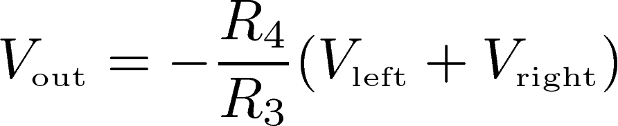
Finally, choosing R3=1kΩ and the adjustable resistor R4 from 0 to 100kΩ allows to bring the signal level to a suitable value that can be displayed by the bargraphs.
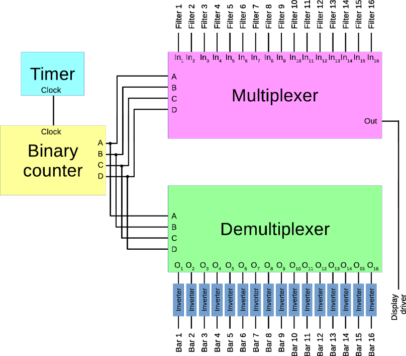
This part of the circuit sequentially selects the output of a given filter, and sends it to the display driver. At the same time, the circuit sends the supply voltage to the corresponding bargraph. This is done by using four integrated circuits: A 16-line multiplexer, a 16-line demultiplexer, a timer, and a 4-bit binary counter. The functional diagram is shown below:
The timer generates a square signal that oscillates between nearly 0V to nearly 5V. This is done by using the NE555 integrated circuit, as shown below:
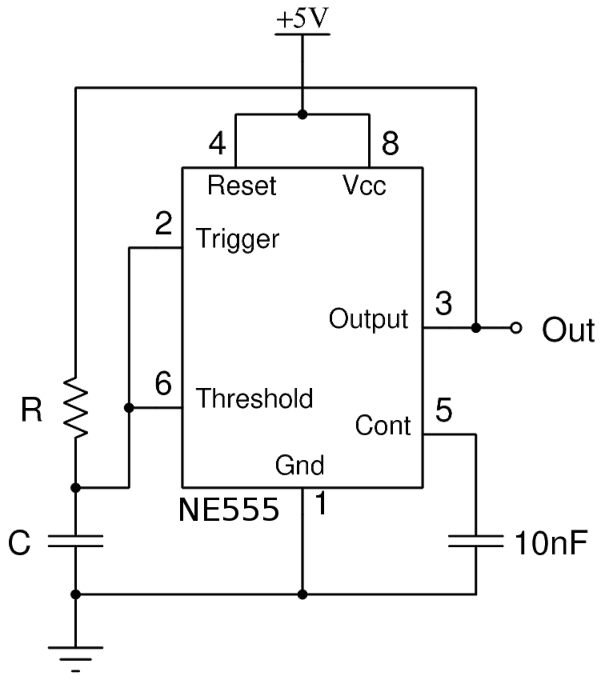
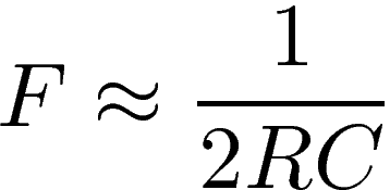
The NE555 works as follows: When the trigger voltage falls below 33% of Vcc the output goes high, when the threshold voltage rises above 67% of Vcc the output goes low. By connecting a capacitor C and a resistor R as shown, the circuit generates a square wave. Initially, the capacitor C is discharged, the trigger voltage is low, and therefore the output is high. Then the capacitor charges across the resistor, until the threshold reaches a high enough potential and resets the output to a low value. The capacitor then discharges across the resistor, until the trigger detects a low voltage and flips the output back to a high level, and the cycle keeps going on. Knowing that the typical time needed for a capacitor to charge or discharge across a resistor is τ=RC, we can estimate, without the need of any precise calculations, that the frequency of the square wave generated is roughly:
This frequency is the frequency at which the circuit switches between the different bargraphs. This frequency must be high enough so that our persistence of vision gives us the illusion that the bargraphs are continuously on. It is commonly accepted that 30 images per second is sufficient to give this illusion. Here we can arbitrarily choose to double this value, and have each bargraph turned on and off 60 times per second. Since there are 16 bargraphs, this means that the frequency must be 960Hz. Using R=47kΩ and C=10nF satisfies this requirement. The additional 10nF capacitor between pins 1 and 5 is recommended by the constructor for the stability of the circuit.
The clock signal generated by the timer is then used to control a 4-bit binary counter. For this, we can use the HC393 integrated circuit that includes two 4-bit binary counters (we use only one). Each time a new clock signal is received, the counter is incremented by one. the output of the counter is denoted by A,B,C,D, where A is the least significant bit (LSB) and D is the most significant bit (MSB). As a result, there are 24=16 possible values for the counter, from 0000 to 1111. When the value is 1111, a further clock signal brings it back to 0000.
The binary value is sent to a 16-line multiplexer and a 16-line demultiplexer, for which we use the HEF4067 and HC154 integrated circuits, respectively. The multiplexer selects one of its 16 inputs (In1, ..., In16), depending on the binary value (the address of the input), and outputs it so it is available for the display driver. The demultiplexer has 16 outputs (O1, ..., O16) that are in a high level state, except the one whose address corresponds to the binary value which is in a low level state. The values of these outputs are inverted by using PNP transistors and used to supply the bargraphs. As a result, only the bargraph that corresponds to the filter selected by the multiplexer is supplied with current and displays the corresponding level.
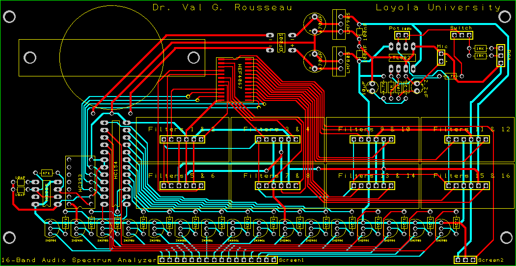
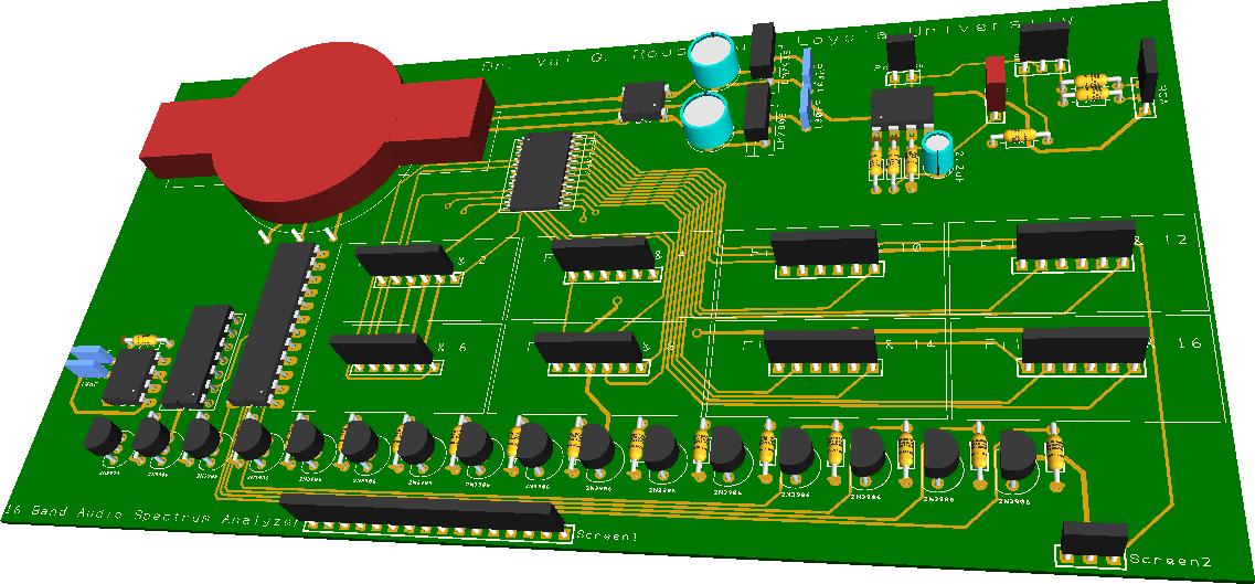
The power supply, the audio mixer, and the multiplexer/demultiplexer unit can be built on the same board. The filters and the display are then plugged to it. The final schematic, PCB image, and 3D preview of the main board are shown below:
Not sure you want to subscribe? Take a peek at the description of the Blue Moonshine channel to get an idea of its contents.